Outline
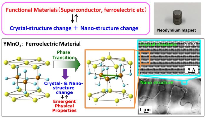
Physical properties of a material are determined by the arrangement of atoms (crystal structures) and their defects (nano- structures). We have studied on the crystal structures and nano- structures in various functional materials such as superconductors, dielectrics, and magnets by mainly transmission electron microscopy (TEM) and X-ray diffraction techniques. TEM is a very powerful tool to magnify materials from several hundred times to one million times (or more), which allows us to directly observe from atomic scale to nano- scale. We can also simultaneously investigate crystal structures by using electron diffraction. With the combination of X-ray diffraction, we are clarifying the origin of emergent phenomena in novel materials and exploring unprecedented functional materials.

<Research Topics>
- Low-temperature structural phase transitions associated with superconductivity in high-Tc superconductors
- Nano- structure changes in high-Tc superconductors
- Improvement the superconducting transition temperature by controlling the local structure of high-Tc superconductors
- Crystal structure changes due to charge-ordering phase transitions in strongly-correlated electron material CuIr2S4
- Dielectric properties and local structures in relaxor ferroelectrics PbTiO3-PbZrO3
- Development of emergent hard magnet by control of nano- structures in Mg(Fe,Mn)2O4
- Characteristic nano- structures in multiferroic RMnO3
- Development of AI hardware devices by ferroelectric RMnO3
- Development of semiconductors by introducing carriers into insulating or ferroelectric materials
etc..
